Semiconductors are constantly in the news as the drive for higher abilities in ever reducing plan sizes. With the statement of 3nm node gadgets entering into production, the obstacles continue to increase. TSMC has actually begun a pilot production of 3nm gadgets[Ref. 1] The shrinking in size is at the point where there are requirements for brand-new transistor styles. The instructions seems moving from FinFET to a Gate-All-Around FETs style. Figure 1 is from referral 2.
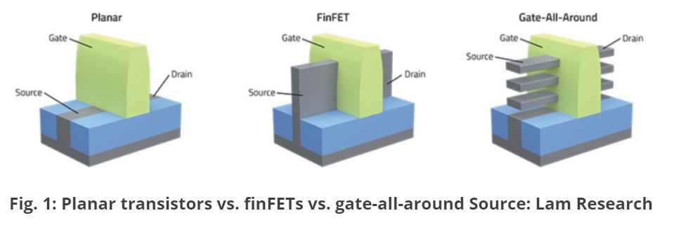
Clearly, there are producing obstacles. Among the proposed GAA FET styles is based upon nanosheets of product. It appears that some makes will present the nanosheet FET at 3nm and others at 2nm. (More information on the advancement of the FETs can be discovered in referral 2.)
Research Study at Tsinghua University in Beijing, China have actually established a transistor with atomically thinned channels that have a gate length of 0.34 nm. [Ref. 3 & 4] This is still years from producing possibilities if it occurs at all. Numerous innovations are established, however a really restricted number have the ability to be established where the procedure would operate in volume production. Nevertheless, this work suggests there a possibilities for ongoing decrease in the size of the transistors.
Scientists at Georgia Tech, Tianjin University, and Kwansei Gakuin University have actually shown a nanoelectronics platform based upon graphene[Ref. 5] The procedure uses e-beam lithography to link the edges to silicon carbide gadgets. If oxygen can link to the graphene, it ends up being graphane, which is an insulator.
There are other choices for enhancing the efficiency abilities of the semiconductor gadgets. Chiplets [Ref. 6] are little components of a circuit that can be utilized throughout a big range of gadgets. The benefits of chiplets consist of the capability of co-locating processors with memory right away surrounding. This lowers the time it takes a signal to relocate to or from memory, which leads to enhanced efficiency. However, absolutely nothing lacks obstacles. Referral 7 covers the requirement for heterogeneous combination to produce multi-die bundles. The benefit of smaller sized location die/chips offers the capability to increase yields due to less intricate private semiconductor functions.
There is another factor to consider when stacking chiplets. A single semiconductor die is developed into a bundle that dissipates heat to keep the gadget temperature level from ending up being too hot. Stacking several chiplets gets rid of these parts of the circuitry far from a heat sync. The accumulation of heat will affect efficiency and might have a negative influence on long-lasting gadget dependability.
All of the efforts within the semiconductor market and scientists worldwide has coordination. In the 1990s, the International Innovation Roadmap for Semiconductors (ITRS) was established to supply assistance for scientists to deal with future requirements that would be needed to be in production over the next 10 to 15 years. This roadmap was upgraded each year. The roadmap committee reorganized the ITRS format to deal with 7 various innovation locations. The roadmap was relabelled the International Roadmap for Gadgets and Systems (IRDS) to more properly deal with the requirements of the total procedure. The duty of the IRDS was moved from the roadmap committee to the Institute of Electrical and Electronic Engineers (IEEE). The focus of the IRDS is still the requirements for the next fifteen years on a constantly moving basis. More information and the roadmap are readily available is referral 8.
Modifications are concerning semiconductor innovation that will enhance the efficiency of gadgets and produce brand-new chances for innovate items that need higher computing power.
Referrals:
- https://auto.economictimes.indiatimes.com/news/auto-components/tsmc-begins-pilot-production-of-3nm-chips/88071568
- https://semiengineering.com/new-transistor-structures-at-3nm-2nm/
- https://www.tomshardware.com/news/semi-transistors-atom-thick
- https://www.nature.com/articles/s41586-021-04323-3
- https://www.graphene-info.com/researchers-take-step-towards-graphene-electronics
- November 2022 Blog Site http://www.nano-blog.com/?m=202211
- https://semiengineering.com/heterogeneous-integration-co-design-wont-be-easy/
- https://irds.ieee.org